

Thin film deposition technique.
- Cecil Cherian

- Jun 17, 2020
- 4 min read
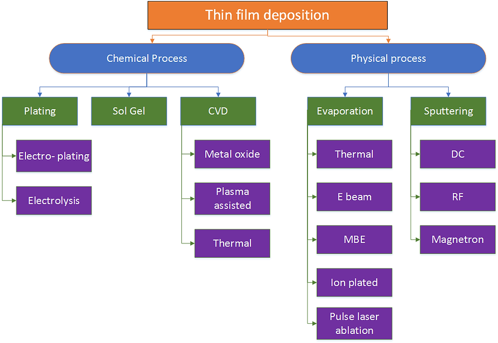
Thin films are layers of material ranging from few atomic layers to 10`s of micrometers. Controlled application of material in this thickness range is achieved by technology known as thin film deposition. There are wide varieties of thin film deposition techniques but all of them can be classified into two broad groups: Physical vapour deposition or PVD and Chemical vapour deposition or CVD. The basic difference lies in the fact that in PVD the vapour phase contains the atoms or molecules to be deposited and these vapours condense onto the required substrate to form a thin film, whereas in CVD the vapours of the constituents undergo a chemical reaction when deposited on the substrate to give the final thin film. Some examples of PVD techniques are: thermal evaporation, e beam evaporation, magnetron sputtering, pulsed laser ablation etc. and some examples of CVD techniques are: thermal CVD, plasma enhanced CVD, metal oxide CVD, atomic layer deposition. Each technique has its own advantages and disadvantages and selecting a deposition technique depends the required film characteristics. For further information on some of these advantages and disadvantages, readers are encouraged to check materials available on the internet such as: (https://www.aimspress.com/fileOther/PDF/Materials/matersci-06-02-174.pdf.) Magnetron sputtering was the technique of choice for thin film deposition for this project because of precise control over deposition rate, thin film structure and chemical composition.
Sputter deposition is carried out in a high vacuum environment, in which targets made of the intended materials are loaded onto cathodes and prepared substrates are kept facing the target material. After achieving the intended vacuum level, high purity Ar gas is introduced into the chamber. Thereafter a high potential difference is applied between the chamber and the target cathode. This strips the electron from the Ar molecules and converts them to Ar+ ions and forms a plasma cloud of these ions. Ar ions from the plasma cloud are accelerated towards the target surface and on impact with the target surface, the Ar ions eject out the target molecules. This continuous bombardment of the target surface leads to the formation of a stream of target species in the plasma plume. These streams of target material then travel towards the substrate and get deposited on the surface. As more and more target species arrive at the substrate surface, they start the film growth on the surface. There are three main mechanism for film growth: Layered growth (Frank Van Der Merwe growth), island growth (Volmer-weber growth) or mixed structure (Stranski-Krastanov growth). One of the main disadvantages of the sputtering technique is its slow deposition rate. Magnetron sputtering is a technique by which the deposition rate of target materials can be increased by creating a precise magnetic field to trap bombarding particles closer to the target surface, leading to a higher collision rate. Depending upon the type of potential difference applied on the cathode, magnetron sputtering can be categorised as: DC sputtering or RF sputtering. DC sputtering is beneficial for conducting targets which can easily dissipate the incoming ions to keep the sputtering process going. But for non-conductive materials, RF sputtering is used because the alternating potential will allow time for dissipation of the accumulated charge to keep the process going. The main advantage of magnetron sputtering compared to other PVD techniques is that it can be used efficiently for metals like Titanium which with high melting points. High density films with very good surface finish can be achieved with magnetron sputtering and it provides very high deposition rate.
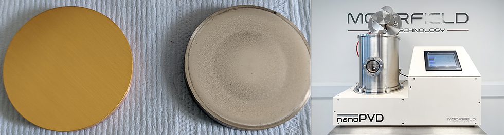
For this project, the 99.99% pure Gold (Au) and Titanium (Ti) targets were procured from the target suppliers. Moorefield`s NanoPvd sputter deposition system was used to perform the thin film depositions, it is a very capable sputter deposition system with all round capabilities. This system contains two sources: 1 DC and 1 RF to load sputtering targets facing up towards the lid of the chamber. Substrates are loaded onto a holder plate attached to the lid of the chamber and are shielded by a shutter which can be opened and closed to allow deposition. Substrate can be rotated to allow uniform deposition of thin films on their surface. There is provision for substrates to be heated up to 600°C when performing the deposition. The Ti target was loaded onto the DC magnetron and Au target was loaded onto RF magnetron. It is known that Ti has a very slow deposition rate compared to Au, therefore, Au was loaded onto RF source to slow down its deposition rate. Prepared glass and Ti substrates were loaded onto the substrate holding plate and the chamber was evacuated to a vacuum pressure better than 0.5 mPa. High purity Ar gas was plumbed into the system. To deposit pure Ti thin films, only the DC source was powered on and to achieve a pure Au film, only the RF source was powered on. After powering the required sources, the substrate shutter was opened to allow the plasma plume to be in direct line of sight with the substrate surface. To make an alloy of Ti-Au system both sources were powered on simultaneously and six different compositions of Ti-Au films were deposited by varying the power on the DC and RF sources. Each deposition lasted 20 minutes and the substrate was rotated at a constant speed of 5 rpm. No substrate heating was employed at this stage of the project but it is planned for future depositions. After the deposition run, the power to the sources was disconnected and the chamber was vented to atmospheric pressure, and the thin film deposited substrates were removed from the substrate holder. Kapton tape attached to glass substrate was peeled off to reveal the step formed between the glass surface and thin film surface. This step could be later used to measure the thin film thickness. Thin film deposited substrates were safely stored in a cleaned microscope slide box to prevent contamination from the environment during transportation.
Deposited thin film samples were then taken for structural, chemical, morphological, mechanical and biological characterization. Visit us again to read about more about the characterization techniques used in this project….


Comments